|
|
Electronics 1
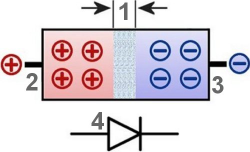
| 1 | boundary layer |
| 2 | p-doped layer |
| 3 | n-doped layer |
| 4 | circuit symbol |
If you are looking for the beginning or core of electronics, then you don't have to travel far. You'll find what you're looking for very quickly, specifically in components that have a pn or np junction. Everything up to
that point, e.g. resistors, capacitors and inductors, can be described as part of the electrical system.
It starts with knowledge of diodes, but it doesn't stop there. Is there even an end in sight when using transistors, their relatives and designs, for example in a fully integrated form and thus into a kind of
underworld of millions of circuits on the surface of a fingernail up to quantum technology?
From the beginning one must probably accept the world as one without electricity. Ions are only created when energy is supplied to the atoms. If they contain more electrons than protons, they are negatively
charged, and if they contain fewer, they are positively charged. It's crazy that we call the places left by electrons 'holes'. The term 'defect electrodes' would be much more meaningful.
And just like the electrons, they are allowed to move, increase or decrease. Regions with more holes are called 'p-type' and those with more electrons are called 'n-type'. A 'diode' is created when two different
areas come into contact with each other. It's best to imagine that p-material directly abuts n-material. It is precisely this area that should be of particular interest to us now.
From now on we call the two areas n- and p-doped. The latter means, for example, the introduction of foreign atoms. If, for example, trivalent boron is introduced into the metal-typical lattice structure, an electron
is missing on the outermost shell, which results in p-doping. Conversely, 5-valent phosphorus, for example, has one electron too many compared to silicon, which leads to n-doping.
This is referred to as targeted contamination of the silicon. You can also use aluminum, indium or gallium instead of boron and antimony or arsenic instead of phosphorus. In this close proximity to each other,
electrons from the p-type semiconductor move into the n-type semiconductor and vice versa, the places left by electrons, therefore called holes or defect electrodes, move into the p-type semiconductor. One
also speaks of diffusion, which means something like penetration.

The once neutral boundary layer is expanding and is now referred to as the 'space-charge region'. However, the one penetrated by the n-region is not directly next to it, but next to the p-region due to the
attraction of different poles. The same also applies to the part of the space-charge region that has become predominantly positive and is now found near the n-region.
A kind of bulwark is created, the famous exclusion zone said to be a classic diode, which becomes larger the more charge carriers are available for the process of building a boundary layer called
'recombination'. However, their blocking effect then increases, which prevents the further movement of (defect) electrons. One then speaks of a kind of equilibrium state.
This occurs earlier with less doped materials and later with more heavily doped materials. It's clear if you remember that n-doping is the application of foreign atoms and p-doping is the creation of a lack of them.
On the one hand, the size of the barrier layer depends on their intensity and, on the other hand, the voltage created by the space charges, also called 'diffusion voltage'.
This can be influenced by a direct voltage. If you put plus on the p-side and minus on the n-side, the resulting electric field reduces this diffusion voltage. The barrier layer becomes smaller as the voltage
increases. With the germanium diodes used in the past, the blocking effect is eliminated at approx. 0.4 V, and with the silicon diodes that are only used today, the blocking effect is eliminated at approx. 0.7 V.
All that remains is reversing the polarity, which, by the way, when operated at high voltage without resistance, destroys a normal diode. If you increase the voltage slowly, you get to know the blocking range,
which extends up to 250 V, for example. So-called Zener diodes are better suited for the blocking range, which, despite similar behavior in the forward direction, are operated exclusively in the reverse direction
and whose reverse current then increases very quickly at certain voltages.
Zener diodes are more commonly used as voltage regulators, while normal diodes are used as rectifiers. This is where their name comes from, with the 'Di' coming from the 'two' in Latin and the 'ode' probably
coming from 'electrode'. The arrow indicates the direction of transmission in which, as an additional advantage, they have very low resistance.
|
|